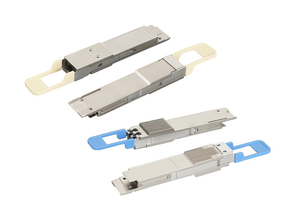
Optical module structural parts
Optical module structural parts
The structural components of an optical module achieve bidirectional conversion between electrical and optical signals through the collaborative work of optoelectronic devices, functional circuits, and optical interfaces. Its working process can be divided into two core links: electro-optical conversion at the transmitting end and electro-optical conversion at the receiving end. The specific details are as follows:
I. Working Process of the Transmitting End (Electrical signal → optical Signal)
Electrical signal input and drive processing
External devices (such as switches and routers) send electrical signals of specific bit rates to the optical module through electrical interfaces.
The electrical signal first enters the driver chip in the functional circuit, where it undergoes shaping, amplification and timing adjustment to ensure that the signal quality meets the requirements for laser driving.
Key technologies: The driver chip needs to support multiple rates (such as 155Mb/s to 2.67Gb/s) and have an automatic power control (APC) function. It compensates for the changes in the laser threshold current by monitoring the backlight current to maintain the stability of the output optical power.
Laser modulation and optical signal generation
The processed electrical signals drive semiconductor lasers (such as VCSEL, DFB, EML, etc.) to emit modulated optical signals that match the telecommunication number rate.
Modulation method: Direct modulation (IM) or electro-absorption modulation (EAM), which achieves optical intensity modulation by changing the injection current of the laser or the electric field intensity of the absorption layer.
Wavelength selection: Depending on the transmission distance and the type of fiber, the wavelength of the laser is typically 850nm (short-wavelength window, multimode fiber), 1310nm/1550nm (long-wavelength window, single-mode fiber).
Optical signal coupling and output
The generated optical signal is focused and coupled to the optical fiber interface (such as LC, SC, MPO, etc.) through optical isolators (to prevent reflected light from interfering with the laser), coupling lenses and other optical components.

Coupling technology: Due to the small core diameter (9μm) of single-mode optical fibers, lens focusing coupling is required. Multimode fibers can be directly coupled through surface-emitting lasers (VCsels).
Ii. Workflow of the Receiving End (Optical signal → Electrical Signal)
Optical signal input and coupling
The optical signal transmitted by the optical fiber enters the optical module through the optical interface, is focused by the coupling lens, and then illuminates the photosensitive surface of the photodetector (such as a PIN photodiode or an APD avalanche photodiode).
Convert optical signals into electrical signals
The photodetector converts the optical signal into a weak current signal, whose intensity is proportional to the incident light power.
Detector type selection
PIN detector: Suitable for short-distance and low-rate scenarios, it features low cost and fast response speed.
APD detector: It enhances sensitivity through avalanche multiplication effect and is suitable for long-distance, high-speed transmission (such as 40G/100G modules).
Electrical signal amplification and processing
The weak current signal first enters the transimpedance amplifier (TIA), where it is converted into a voltage signal and initially amplified.
The limiting amplifier (LA) further shapes and controls the gain of the signal, eliminates noise interference, and restores a clear electrical signal.
High-speed signal processing: In 400G/800G modules, the DSP chip performs dispersion compensation, clock recovery and bit error correction on the signal to ensure signal integrity.
Electrical signal output
The processed electrical signal is output to the external device through the electrical interface, completing the entire process of photoelectric conversion.
Iii. Key Performance Assurance Technologies
Temperature compensation and stability control
The bias current and modulation current of the laser are dynamically adjusted through digital potentiometers or K-factor compensation methods to compensate for the influence of temperature changes on optical power and extinction ratio.
Table lookup method: The controller, based on the feedback value of the temperature sensor, looks up the table to adjust the resistance value of the digital potentiometer, achieving precise control of the modulated current.
Signal integrity optimization
An RC matching circuit is designed between the driver and the laser to reduce signal reflection and loss and improve the quality of high-speed signal transmission.
The feedforward equalization (FFE) or decision feedback equalization (DFE) technology is adopted to compensate for the dispersion and loss of optical fibers and extend the transmission distance.
Low-power design
By adopting linear drive pluggable (LPO) or photoelectric co-packaging (CPO) technology, the power consumption of DSP chips is reduced and energy efficiency is improved.
Optimize the circuit design, reduce static power consumption, and meet the high-density deployment requirements of data centers.
Ding Dong:+86 136-2094-9831


Douyin
Copyright © 2025 Dongguan Laoyou Hardware Products Co., Ltd. All rights reserved
The webpage materials and related resources of this site are all from the Internet. If there is any infringement, please inform us immediately and we will delete it within 24 hours.