
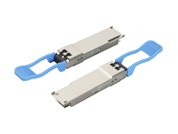
Optical module structural parts
Optical module structural parts
The output stage of optical module structural components is the final phase of the process for converting optical signals into electrical signals. Its core task is to stably output the processed signals in a standard format to external devices while ensuring that the signal quality meets the system requirements. The following is a detailed description from the two directions of optical output at the transmitting end and electrical output at the receiving end, combined with key technical details:
I. Optical output link at the transmitting end
The final formation and coupling of optical signals
Optical path design
The optical signal emitted by the laser needs to pass through an optical isolator (to prevent reflected light from interfering with the stability of the laser), a wavelength selection element (such as a filter or grating to ensure that the wavelength meets the standard), and a coupling lens group.
Single-mode fiber coupling: As the core diameter is only 9μm, high-precision lenses (such as aspheric lenses) are required to focus the light spot to the center of the core, and the coupling loss is usually controlled within 0.5dB.
Multimode fiber coupling: VCSEL lasers can be directly coupled through surface emission, with relatively low losses (about 1-2dB), but it is necessary to control the mode field matching to avoid intermode dispersion.
Standardization of optical interfaces
The output end of the optical module adopts standard interfaces (such as LC, SC, MPO), and mechanical alignment is achieved through ceramic sleeves or metal flanges to ensure the stability of physical connection with external optical fibers.
MPO interface: It is used for high-density parallel transmission (such as 400G/800G modules), supporting 12-core or 24-core fiber arrays. The end face flatness must be ensured through precise crimping process.
2. Optical power control and monitoring
Automatic Power Control (APC)
The driver chip monitors the current of the laser backlight diode (MPD), adjusts the bias current and modulation current in real time, and compensates for the fluctuations in optical power caused by temperature changes or device aging.
Closed-loop control: The APC circuit uses the MPD current as the feedback signal and dynamically adjusts the drive parameters through the PID algorithm to ensure that the output optical power is stable at the target value (such as -3 DBM to +3dBm).
Optical power alarm function
The module is equipped with an optical power monitoring circuit. When the output optical power is lower than the threshold (such as -12 DBM) or higher than the overload point (such as +7dBm), an LOS (Loss of Signal) alarm is triggered to notify the system to perform protection switching or fault location.
3. Quality assurance of optical signals
Extinction ratio (ER) optimization
By adjusting the ratio of the modulation current to the bias current of the laser, ensure that the optical power ratio (ER) of all "1" codes to all "0" codes meets the standard (such as ≥3.5dB), and avoid code errors caused by insufficient signal contrast.
Temperature compensation: ER may decrease as the temperature rises, and the modulation parameters need to be dynamically adjusted through table lookup or linear compensation algorithms.
Spectral characteristic control
For DWDM (Dense Wavelength Division Multiplexing) modules, the spectral width of the laser (such as ≤0.1nm) must be strictly limited through gratings or filters to prevent crosstalk between adjacent channels.
Ii. Electrical Output Link at the receiving end
Amplification and shaping of electrical signals
Transimpedance amplifier (TIA
Convert the weak current signal (μA level) output by the photodetector into a voltage signal (mV level) and initially amplify it. TIA needs to have low noise and high bandwidth characteristics to support the transmission of high-speed signals (such as 25G/50G).
Noise optimization: By adopting a common-source common-gate structure or feedback resistor tuning technology, the input reference noise (RIN) is reduced and the signal-to-noise ratio (SNR) is improved.
Limiting amplifier (LA)
The voltage signal output by the TIA is further amplified and shaped to eliminate noise interference and signal jitter, and a standard logic level (such as CML or LVDS) is output.
Automatic Gain Control (AGC) : LA can dynamically adjust the gain according to the input signal strength to ensure that the output amplitude remains stable within the target range (such as 800mVpp).
2. High-speed signal processing and equalization
Feedforward equilibrium (FFE)
Integrate a digital equalizer at the back end of LA and compensate for the attenuation of high-frequency signals through pre-emphasis technology to improve the quality of the eye map. For instance, in a 40G PAM4 signal, FFE can increase the signal margin by more than 20%.
Decision Feedback Equilibrium (DFE)
For long-distance transmission (such as over 80 kilometers), DFE eliminates inter-symbol interference (ISI) through feedback loops, further reducing the bit error rate (BER).
DSP integration: In 400G/800G modules, the DSP chip integrates FFE, DFE and clock data recovery (CDR) functions to achieve fully digital signal processing.
3. Standardization of electrical interfaces and signal integrity
Electrical interface type
According to the rate and protocol requirements, the electrical output interface can adopt the CML differential signal of SFP+, the LVDS of QSFP-DD or the PCIe PHY standard of PCIe.
Impedance matching: The electrical interface needs to be designed with a 50Ω differential impedance, and signal integrity should be achieved through PCB lamination optimization and termination resistance.
Signal Eye Diagram optimization
By adjusting the driving current, pre-weighting coefficient and balancing parameters, ensure that the eye diagram opening degree of the electrical output signal meets the standards (such as eye height ≥300mV, eye width ≥0.7UI).
4. Electrical signal monitoring and protection
Eye Monitor:
The module is equipped with an internal eye diagram analysis circuit to monitor the output signal quality in real time and report parameters such as bit error rate and jitter to the system through the I2C interface.
Adaptive equalization: Based on the monitoring results of the eye diagram, dynamically adjust the FFE/DFE parameters to optimize signal quality.
Electrostatic Protection (ESD)
The electrical interface adopts TVS diodes or ESD protection arrays to prevent human static electricity or equipment surges from damaging the internal circuits of the module.
Iii. Typical Application Scenarios in the Output Stage
Data Center Interconnection
The 400G QSFP-DD module outputs 8 channels of 50G PAM4 optical signals through the MPO interface, which are transmitted to the opposite end device via optical fiber. The electrical output end needs to support PCIe 5.0 or Ethernet protocol.
The output optical power needs to match the fiber loss to ensure that the transmission distance reaches 10km (SR4) or 40km (DR4).
5G fronthaul network
The 25G SFP28 module outputs NRZ optical signals through the LC interface. The electrical output terminal needs to be compatible with the eCPRI protocol, and the delay needs to be controlled within 10μs.
The output extinction ratio needs to be ≥6dB to meet the high-sensitivity reception requirements of wireless base stations.
Long-distance transmission system
The 100G CFP2-DCO module outputs DWDM optical signals through an adjustable laser. The electrical output terminal needs to integrate a DSP chip to support FEC error correction and soft decision decoding, reducing the bit error rate to below 10^-15.
Iv. Future Trends in the Output Link
Silicon photonics integration
Integrate the laser, detector, TIA/LA and DSP onto a silicon-based chip to reduce the module size and lower power consumption (for example, the power consumption of a 400G silicon photonic module is less than 6W).
Silicon optical coupling technology (such as grating couplers) can simplify the optical fiber docking process and enhance production efficiency.
Co-packaged Optics (CPO)
The optical module is co-packaged with the switch ASIC chip to shorten the transmission distance of electrical signals, reduce power consumption and delay (for example, the power consumption of an 800G CPO module is less than 10W).
The electrical output link needs to adopt a high-speed SerDes interface (such as 112G PAM4) to support optical interconnection between chips.
Intelligent management
Integrate temperature sensors, optical power meters and microcontrollers to achieve real-time monitoring and adaptive adjustment of output parameters.
Predict the lifespan of devices through AI algorithms, trigger maintenance processes in advance, and enhance system reliability.
The output link of optical module structural components is the "last mile" of optical communication systems, and its performance directly determines the reliability and efficiency of signal transmission. Through continuous innovation in optical coupling optimization, high-speed signal processing and intelligent management technologies, optical modules are evolving towards higher speeds, lower power consumption and smaller size, providing key support for emerging fields such as 5G, data centers and artificial intelligence.
Ding Dong:+86 136-2094-9831


Douyin
Copyright © 2025 Dongguan Laoyou Hardware Products Co., Ltd. All rights reserved
The webpage materials and related resources of this site are all from the Internet. If there is any infringement, please inform us immediately and we will delete it within 24 hours.

