
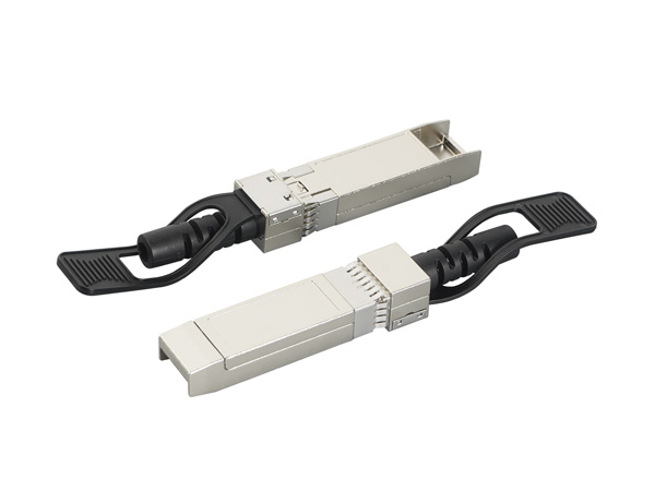
Optical module structural parts
Optical module structural parts
The key technologies of optical module structural components cover multiple aspects such as photoelectric conversion, packaging design, material innovation, high-frequency signal processing, and power consumption optimization. These technologies jointly support optical modules in achieving efficient and stable photoelectric signal transmission. The following is the specific introduction:
I. Photoelectric Conversion Technology
Photoelectric conversion is the core function of optical modules, mainly achieved by the optical transmitting component (TOSA) and the optical receiving component (ROSA).
Optical Emission Assembly (TOSA)
Light source: Laser diodes (LD) or light-emitting diodes (LED) are adopted. Among them, LD has the advantages of low power consumption, high power and high coupling efficiency, and is the mainstream choice.
Drive circuit: Processes the input electrical signal and drives the light source to emit modulated light signals of the corresponding rate.
Optical power automatic control circuit: Ensures that the output optical signal power remains stable and enhances transmission reliability.
Optical receiving component (ROSA)
Photodetector: It converts the received optical signal into an electrical signal. Common types include PIN photodiodes and avalanche photodiodes (APD). APD has an internal gain mechanism that can enhance sensitivity and is suitable for long-distance transmission.
Signal processing circuit: It includes a preamplifier and a limiting amplifier, which amplify and process the converted electrical signal and output an electrical signal of the corresponding bit rate.
Ii. Packaging Technology
Packaging technology has a significant impact on the performance, reliability and cost of optical modules.
Airtight packaging
Objective: To prevent external moisture and harmful gases from entering the interior of sealed optical devices, which could affect the performance of optical chips and related components.
The methods include To-can, BOX (box type), butterfly packaging, etc. They are mainly applied in the telecommunications market or DCI market (long-distance transmission in data centers) where the working environment is complex and reliability requirements are high.
Non-airtight packaging
Objective: To reduce costs and enhance production efficiency.
The main method is COB (Chip on Board) packaging technology, which is mostly used for optical modules in data centers. COB packaging directly installs the chip on the printed circuit board, connecting the chip pins to the contact points of the printed circuit board with gold or copper wires. It has the advantages of small size, light weight, high reliability and low cost.
Iii. Material Innovation
Material innovation is the key to improving the performance of optical modules.
Optical chip material
Laser chips can be classified into surface-emitting chips (such as VCSEL) and edge-emitting chips (such as FP, DFB and EML chips) based on their light-emitting structure. Optical chips made of different materials have distinct performance characteristics and are suitable for various application scenarios.
Detector chips: There are mainly two types, PIN and APD. Among them, APD chips enhance detection sensitivity through the avalanche multiplication effect.
Encapsulation material
Dielectric materials: The dielectrics used in airtight packaging are generally non-organic materials, such as glass or ceramics, to ensure reliable sealing of the packaging.
Optical materials: including lenses, filter plates, etc., are used to optimize optical path coupling and signal transmission. Lenses can be classified into spherical and aspheric types based on their shapes, and by material, they mainly include glass, silicon, plastic, etc.
Iv. High-frequency Signal Processing Technology
With the continuous increase in the speed of optical modules, high-frequency signal processing technology has become particularly important.
PAM4 modulation technology
Principle: Higher bandwidth is achieved by enhancing the symbol rate. For instance, the 4×200G PAM4 solution can support single-mode fiber transmission of 800G optical modules.
Advantage: Compared with the traditional NRZ modulation technology, PAM4 modulation technology can transmit twice the amount of data under the same bandwidth.
Related technology
Principle: Utilizing coherent light (light waves with the same frequency and fixed phase relationship) for signal transmission and processing, it supports complex modulation, demodulation, and signal processing functions.
Application: Coherent optical modules are widely used in 100G and ultra-100G rate communication scenarios, such as long-distance backbone, metropolitan area, access, DCI networks, etc.
V. Power Consumption Optimization Technology
Power consumption optimization is an important direction in optical module design, especially for high-speed and high-density optical modules.
Silicon photonics technology
Principle: By using silicon-based substrate materials and integrating lasers, modulators and detectors through CMOS technology, the number of components is reduced and costs are lowered.
Advantages: Silicon photonic modules have the advantages of low power consumption and high integration, and are suitable for power-sensitive application scenarios such as data centers.
CPO (Optoelectronic Co-Packaging) technology
Principle: Co-package the optical engine and the switching chip to shorten the transmission distance and reduce power consumption.
Application: CPO technology is expected to be commercially available in the coming years, providing core support for AI computing power and data centers.
Ding Dong:+86 136-2094-9831


Douyin
Copyright © 2025 Dongguan Laoyou Hardware Products Co., Ltd. All rights reserved
The webpage materials and related resources of this site are all from the Internet. If there is any infringement, please inform us immediately and we will delete it within 24 hours.

